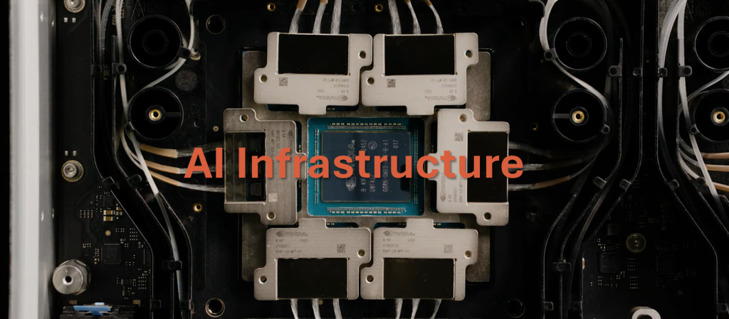

AI infrastructure stocks have become the focus of every investor in 2025, with the narrative simple: buy the companies building the data centers, making the chips, and selling the shovels. But beneath the trillion-dollar data center buildout lies a more nuanced reality where some AI infrastructure stocks generate compounding returns while others face structural headwinds that no amount of AI demand can overcome.
Currently, the challenge isn’t finding AI infrastructure exposure. It’s separating the technologies experiencing genuine paradigm shifts from those hitting physical limits, cyclical peaks, or commoditization traps.
Quick jump:
- 1 Which infrastructure technologies show sustainable growth trajectories?
- 2 Why is advanced packaging outperforming lithography despite lower headlines?
- 3 How are inference chips disrupting NVIDIA’s dominance?
- 4 How should investors evaluate the memory crisis?
- 5 What are the key patterns separating infrastructure winners from losers?
- 6 What’s the investment strategy for AI infrastructure exposure?
- 7 What’s the bottom line for infrastructure investing in the AI era?
- 8 Q&A
- 9 Get Started Today
Which infrastructure technologies show sustainable growth trajectories?
Among AI infrastructure stocks, three categories demonstrate explosive growth with structural demand drivers: advanced packaging, AI-specific inference hardware, and high-bandwidth memory.
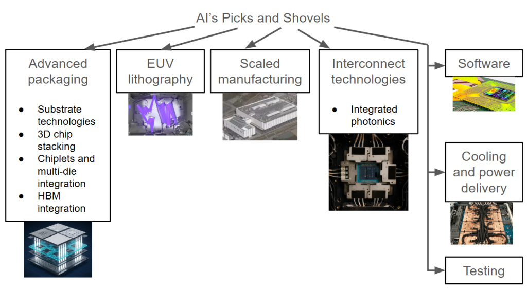
Advanced packaging shows paradigm-shift economics
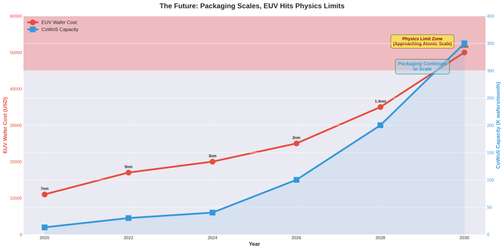
TSMC‘s CoWoS capacity doubled from 35,000 wafers per month (2024) to 70,000 wpm (2025), with 30% expansion planned for 2026. Assembly and packaging equipment grew 19.6% in 2025, outpacing wafer fabrication equipment’s 11% growth
Inference chips demonstrate 28% CAGR
For AI infrastructure stocks, the inference chip market exploded from $31 billion (2024) to a projected $167 billion (2032). More critically, inference workloads now consume two-thirds of all AI compute (up from one-third in 2023). While dedicated inference chip sales are hitting $50+ billion in 2026.
HBM memory shows 600% growth trajectory
High-bandwidth memory surged from $16 billion (2024) toward $100+ billion (2030). SK Hynix captured 62% market share with its entire 2026 capacity already booked. Each new GPU generation consumes larger wafer allocations, creating a zero-sum game against consumer electronics.
Two categories show moderate but profitable growth
Edge AI processors (17.75% CAGR reaching $36 billion by 2034) and testing equipment (surging 48.1% in 2025, driven by complex AI architectures).
Three categories show concerning dynamics despite massive investments
EUV lithography (mature 7.57% CAGR), consumer DRAM/NAND (multi-year decline predicted), and legacy nodes ≥28nm (oversupply and weak demand through 2026).
Why is advanced packaging outperforming lithography despite lower headlines?
AI infrastructure investors should note the most profitable infrastructure bet in semiconductors today, delivering 19.6% annual growth while requiring lower capital intensity than cutting-edge lithography.
The economics of packaging:
TSMC’s CoWoS packaging enables AI chips that would be physically impossible through traditional manufacturing. Each Nvidia H100 requires sophisticated 2.5D packaging integrating GPU dies with HBM memory stacks. When TSMC doubled CoWoS capacity to 70,000 wafers monthly, it couldn’t keep pace with demand, prompting the additional 30% expansion for 2026.
Amkor Technology (AMKR) secured a $1.6 billion CHIPS Act grant to build a $2 billion advanced packaging facility in Arizona, with Apple as anchor customer. The company provides flip-chip, fan-out wafer-level packaging, and system-in-package solutions, exactly the technologies required for AI accelerators.
ASE Technology(ASX), the world’s largest OSAT (outsourced assembly and test), dominates the packaging ecosystem with integrated circuit assembly, testing, and materials capabilities. The company’s exposure to AI packaging, automotive electronics, and IoT positions it at the convergence of multiple growth vectors.
The strategic advantage is structural
While only ASML can sell EUV machines, dozens of companies compete in packaging, but the technology barriers are rising rapidly. Companies mastering chiplet integration, thermal management, and ultra-high-density interconnects are building moats that pure-play foundries cannot easily replicate.
| Metric | EUV/Node Shrinkage | Advanced Packaging |
|---|---|---|
| Equipment Cost per Unit | $220M-$380M (EUV) | $2M-$10M (packaging tools) |
| Total Fab Investment | $15B-$30B (leading edge) | $2B-$5B (packaging facility) |
| Performance Gain | 1.4-1.6x per node | 1.3-1.5x (chiplets + HBM) |
| Development Cost | $500M-$600M+ (5nm/3nm) | $150M-$240M (chiplet design) |
| Time to Market | 36-48 months | 18-24 months |
| Yield Impact | Decreasing (60% at 5nm for large dies) | Increasing (85-94% per chiplet) |
| Scalability | Limited by physics | Highly scalable (add chiplets) |
Compare packaging to lithography
ASML enjoys a monopoly on EUV systems, but growth is constrained to 7.57% CAGR as Moore’s Law slows and marginal gains diminish. Each new node delivers smaller improvements at exponentially higher costs. Advanced packaging, by contrast, enables performance leaps through heterogeneous integration. Advanced packaging is combining chips from different nodes and processes to achieve what single-die scaling cannot.
How are inference chips disrupting NVIDIA’s dominance?
The AI compute market is bifurcating into training (dominated by NVIDIA) and inference (increasingly fragmented), with inference chips growing 28% annually while training infrastructure matures.
OpenAI’s October 2024 announcement crystallized the shift. OpenAI partnered with Broadcom and TSMC to develop specialized inference chips. When the world’s leading AI company designs custom silicon for deployment rather than training, the message is clear: inference economics demand purpose-built hardware.
The financial logic behind inference
Cerebras announced inference speeds of 2200 tokens per second for Llama 3.1 8B, outperforming GPU-based solutions by 20x with 100x better price-performance. Intel’s Gaudi accelerators target inference workloads with competitive performance at lower power consumption.
AMD‘s strategic positioning as the inference challenger gained credibility with MI300 series GPUs offering competitive memory (192GB HBM) and nearly matching NVIDIA’s compute performance, but at potentially lower cost. The company’s forward P/E of ~28x versus NVIDIA’s 32x creates room for multiple expansion if inference revenues materialize.
Hyperscalers accelerated custom chip development: Google‘s TPU v5e optimizes for inference, Amazon‘s Inferentia2 powers cost-effective deployment, and Meta develops MTIA for recommendation models and LLM inference. These chips aren’t replacing NVIDIA in training; they’re capturing deployment economics NVIDIA hasn’t optimized for.
The market dynamics
Training chips still cost $200+ billion in 2026, but inference chip sales hit $50+ billion, growing from essentially nothing three years ago. As inference workloads increase from 50% to 67% of compute by 2026, the margin pressure on general-purpose training GPUs becomes structural, not cyclical.
Groq raised $640 million for Language Processing Units purpose-built for inference. SambaNova, d-Matrix, and Tenstorrent collectively raised over $1 billion in 2024-2025 specifically for inference-optimized architectures. These aren’t experiments; they’re billion-dollar bets that inference will fragment from training hardware.
NVIDIA‘s training monopoly remains intact, but inference deployment is becoming contested territory. Where ASICs, NPUs, and specialized accelerators compete on price-performance rather than raw capabilities.
How should investors evaluate the memory crisis?
The memory market isn’t experiencing a shortage; it’s experiencing permanent reallocation, creating winners in AI infrastructure and losers in consumer electronics with no path to equilibrium.
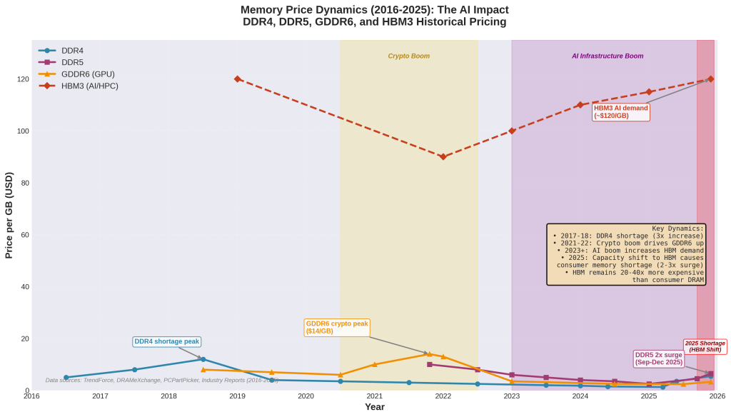
HBM represents the clearest infrastructure bet: SK Hynix booked its entire 2026 capacity before the year began, with 62% market share in the fastest-growing memory segment. Every new GPU generation demands more HBM. Nvidia’s H100 requires HBM3, Blackwell demands HBM3E, and future generations will consume HBM4.
Micron(MU) provides US-based exposure to HBM with 21% market share, critical for customers requiring domestic supply chains. The company’s investments in HBM3E and next-generation packaging position it as the alternative to Korean manufacturers for hyperscalers building US data centers.
Samsung lags at 17-22% market share but offers recovery potential if execution improves. The company’s massive capital resources and integrated manufacturing suggest the gap is operational, not structural, creating a value opportunity if Samsung reaches parity with SK Hynix(000660.KO) in HBM technology.
The strategic reality is zero-sum: HBM growth comes directly at the expense of commodity DRAM and NAND. Samsung, SK Hynix(000660.KO), and Micron(MU) cannot expand total wafer capacity fast enough to serve both markets. Every HBM stack means fewer smartphone memory modules, PC SSDs, or server DRAM.
IDC’s projection of 16% DRAM supply growth and 17% NAND growth in 2026 falls “below historical norms” specifically because cleanroom space shifts toward enterprise AI components. This isn’t temporary; it’s strategic repositioning toward products earning 3-5x higher margins.
For investors, the implication is binary: HBM suppliers win decisively, consumer-focused memory companies lose structurally. Companies like Western Digital or Kingston Technologies serving consumer storage markets face permanent demand reduction, while SK Hynix(000660.KO) and Micron’s(MU) HBM exposure becomes more valuable every quarter.
The memory crisis isn’t a bug; it’s a feature of AI infrastructure economics permanently reshaping semiconductor capital allocation.
What are the key patterns separating infrastructure winners from losers?
After examining technologies from EUV lithography to neuromorphic computing across a $700+ billion market, clear patterns emerge explaining why some infrastructure bets compound while others stagnate.
Infrastructure delivers exceptional returns when four factors align:
Solving AI-specific bottlenecks: Advanced packaging enables chip architectures impossible through traditional methods. HBM eliminates memory bandwidth constraints. Inference chips optimize for deployment economics rather than training performance. Each addresses a constraint that didn’t exist five years ago.
Growing faster than Moore’s Law: Advanced packaging (19.6% growth) outpaces transistor scaling (7.57% lithography growth). Neuromorphic computing (89.7% CAGR) and inference chips (28% CAGR) reflect paradigm shifts, not incremental improvements.
Enabling new architectures, not just faster versions: Chiplets fundamentally change how processors are designed. Optical interconnects replace electrical signaling at the physical layer. Neuromorphic chips process information through spiking neural networks rather than continuous computation. Architectural shifts create moats that capital expenditure alone cannot overcome.
Multiple buyers competing for scarce capacity: TSMC’s CoWoS packaging constrains every major AI chip designer. HBM supply limits GPU production regardless of foundry capacity. Testing equipment sees 48.1% growth because complex AI chips require more sophisticated verification. When demand exceeds supply systemically, pricing power persists.
By contrast, infrastructure investments struggle when:
Serving declining end markets: Legacy nodes (≥28nm) face structural oversupply as China floods capacity. Consumer memory sees permanent demand reduction as smartphones and PCs become lower priorities. Analog ICs grow at a mature 4.8%.
Hitting physical limits that capital can’t solve: EUV lithography delivers diminishing returns below 3nm nodes. Each successive generation costs exponentially more for smaller improvements. ASML’s monopoly creates a ceiling, not a moat, when technology approaches quantum mechanical constraints.
Facing commoditization as technology matures: Traditional DRAM and NAND become interchangeable absent HBM differentiation. Discrete components and microcontrollers compete primarily on price. When any manufacturer can produce equivalent products, margins compress regardless of AI demand.
Cyclical exposure overwhelming secular trends: Agriculture equipment proves AI technology works (59% herbicide reduction), but cyclical collapse erases benefits. Consumer electronics show unit shipment declines overwhelming any efficiency improvements. Cyclicality and secular growth become opposing forces, not complementary ones.
What’s the investment strategy for AI infrastructure exposure?
The counter-intuitive play isn’t buying data center infrastructure broadly, it’s identifying technologies experiencing genuine paradigm shifts while avoiding commoditization traps disguised as AI exposure.
For growth investors focused on compounding technological advantages:
ASE Technology and Amkor Technology provide advanced packaging exposure with 19.6% market growth and structural positioning as AI chip complexity increases. ASE’s OSAT dominance and Amkor’s $2 billion Arizona facility with Apple as anchor customer demonstrate both current leadership and future capacity.
SK Hynix offers pure-play HBM exposure with 62% market share and 2026 capacity already booked. The company’s technology lead in HBM3E and transition to HBM4 creates compounding advantages as each GPU generation demands more sophisticated memory.
Micron provides US-based HBM access critical for domestic data center builds, with 21% market share and expanding production. The geopolitical premium for American memory manufacturing adds strategic value beyond financial metrics.
For value investors seeking overlooked paradigm shifts:
Intel and IBM bury neuromorphic computing divisions within massive corporations. Loihi 3 and NorthPole represent options on 89.7% CAGR markets while trading at broader company valuations. If neuromorphic chips reach commercial scale, these divisions justify significant value creation despite representing tiny revenue percentages today.
AMD positions itself as the inference-chip challenger with the MI300 series, competitive on memory and compute but potentially better priced than NVIDIA. Forward P/E of ~28x versus NVIDIA’s 32x creates multiple expansion opportunities if inference market share materializes.
Broadcom enables custom ASIC development for hyperscalers (Google, Amazon, Meta, OpenAI). Broadcom is designing inference chips, capturing revenue from NVIDIA’s biggest competitors without competing directly in chips.
For contrarian investors, identifying structural misunderstandings:
Testing equipment companies (KLA, Teradyne) show 48.1% growth in 2025, higher than almost any semiconductor category. The growth is driven by AI chip complexity, requiring more sophisticated verification. The market focuses on chip designers while testing becomes a hidden bottleneck.
Optical interconnect startups (Ayar Labs $370M raised, Lightmatter $400M at $4.4B valuation) solve bandwidth constraints that advanced packaging and HBM cannot address. These remain private but represent the next infrastructure bottleneck after memory and packaging.
Cociousness required while considering the following:
- legacy node pure-plays. Regardless of AI rhetoric, the bifurcation between advanced nodes (AI) and mature nodes (consumer) creates permanent structural decline for ≥28nm focused manufacturers.
- consumer memory exposure (Western Digital, Kingston). As permanent reallocation toward HBM eliminates the “cyclical recovery” narrative that historically drove these stocks.
- Betting on EUV lithography growth (ASML suppliers). Beyond current valuations, 7.57% CAGR reflects technological maturity hitting quantum limits, not an artificial constraint waiting to be released.
What’s the bottom line for infrastructure investing in the AI era?
AI infrastructure is transforming semiconductor economics, but not evenly, not predictably, and not always profitably for every component of the stack.
Three main categories show genuine paradigm-shift growth:
- advanced packaging (19.6% with structural demand from chiplet architectures),
- HBM memory (600% growth to 2030, creating winner-take-all dynamics),
- inference chips (28% CAGR displacing general-purpose GPUs in deployment).
These combine architectural necessity, supply constraints, and multiple buyers competing for scarce capacity.
For investors, the most compelling infrastructure opportunities aren’t the most obvious ones. NVIDIA, TSMC, and ASML already trade at valuations reflecting AI dominance. The asymmetric returns appear in advanced packaging companies, enabling impossible chip architectures. HBM manufacturers with 2026 capacity already sold, inference chip challengers fragmenting NVIDIA’s deployment monopoly, and neuromorphic computing hiding 89.7% growth inside larger corporations.
The revolution isn’t happening in data centers alone. It’s happening in TSMC’s CoWoS lines, doubling capacity annually, and SK Hynix’s HBM fabs are booked two years forward.
Q&A
Q: Why focus on infrastructure components rather than complete data center solutions?
A: Complete solutions (Dell, HPE) face margin compression as components commoditize. Component suppliers with technological moats (advanced packaging, HBM) capture value that system integrators cannot extract. SK Hynix’s HBM shortage creates pricing power; Dell’s server assembly does not.
Q: Which infrastructure technologies show the clearest path to sustained margins?
A: Three technologies demonstrate pricing power through scarcity:
- HBM memory (SK Hynix’s entire 2026 capacity booked)
- Advanced packaging (TSMC CoWoS constrained despite doubling capacity)
- Inference chips
Each faces structural demand exceeding supply, regardless of capital investment.
Q: What’s the biggest misconception about AI infrastructure investing?
A: That all infrastructure benefits equally from AI growth. EUV lithography grows at 7.57% (mature technology hitting limits) while neuromorphic computing grows at 89.7% (paradigm shift). Consumer memory declines permanently, while HBM grows 600%. The infrastructure category is bifurcating as dramatically as the applications it enables.
Q: How should investors think about NVIDIA’s competitive position in inference?
A: NVIDIA dominates training (~80% market share), but inference is fragmenting. OpenAI, Google, Amazon, and Meta design custom chips for deployment economics, not training performance. AMD, Intel, Groq, Cerebras, and dozens of startups target inference-specific optimizations. Training remains NVIDIA’s moat; inference is becoming contested territory where ASICs compete on price-performance, not absolute capability.
Q: What AI infrastructure stocks should pay attention?
A: Here is a table with the biggest players among the AI infrastructure stocks:
| Ticker | Name | Tech Category | Key Brands/Products | Investment Thesis |
|---|---|---|---|---|
| ASX | ASE Technology | Advanced Packaging | OSAT services for AI chips | World’s largest OSAT capturing 19.6% annual growth in advanced packaging for chiplets and HBM integration |
| AMKR | Amkor Technology | Advanced Packaging | Flip-chip, fan-out WLP, SiP | $2B Arizona facility with Apple as anchor customer positions for onshore AI chip packaging boom |
| TSM | TSMC | Advanced Packaging | CoWoS, SoIC | CoWoS capacity doubled to 70k wpm with 30% further expansion capturing AI chip packaging bottleneck |
| INTC | Intel | Advanced Packaging | Foveros 3D stacking | Foveros enables heterogeneous integration critical for next-gen AI accelerators and chiplet architectures |
| IMOS | ChipMOS Technologies | Advanced Packaging | Memory and display driver packaging | Specialized packaging for memory and logic benefits from AI-driven DRAM/testing demand |
| ASML | ASML | EUV Lithography | EUV and DUV systems | Monopoly on EUV but growth constrained to 7.57% CAGR as Moore’s Law slows at sub-3nm nodes |
| GFS | GlobalFoundries | Foundry Services | 22nm FDX, 12nm FinFET | Third-largest foundry focusing on mature nodes and specialty processes avoiding bleeding-edge capex race |
| SNPS | Synopsys | EDA Software | Fusion Compiler, 3DIC Compiler | 36-40% EDA market share essential for designing complex AI chips with chiplets and advanced nodes |
| CDNS | Cadence Design Systems | EDA Software | Innovus, Cerebrus | 30-35% EDA market share capturing AI chip design complexity requiring advanced simulation tools |
| VRT | Vertiv | Cooling & Power | Data center cooling infrastructure | Leading data center cooling provider capturing $400B+ annual AI data center capex through 2026 |
| NVT | nVent Electric | Cooling & Power | Thermal management and enclosures | Thermal management solutions for liquid-cooled AI servers burning kilowatts per chip |
| ETN | Eaton | Cooling & Power | Power distribution and liquid cooling | Power management and liquid cooling systems required for dense AI compute racks |
| KLAC | KLA Corporation | Testing & Metrology | Surfscan, eDR7380 | Market leader capturing 48.1% testing equipment growth as AI chip complexity demands sophisticated metrology |
| TER | Teradyne | Testing & Metrology | Automated test equipment | ATE leader benefiting from complex AI chips requiring extensive testing before deployment |
| AMAT | Applied Materials | Testing & Metrology | Metrology and inspection systems | Diversified equipment provider with metrology benefiting from advanced node and packaging verification needs |
| ONTO | Onto Innovation | Testing & Metrology | Optical metrology and inspection | Specialized optical inspection capturing advanced packaging and sub-3nm node metrology demand |
| NVMI | Nova Ltd | Testing & Metrology | Integrated and standalone metrology | Process control metrology for advanced nodes and new materials in AI chip manufacturing |
| 000660.KO | SK Hynix | High-Bandwidth Memory | HBM3, HBM3E, HBM4 | 62% HBM market share with entire 2026 capacity booked capturing 600% memory growth to 2030 |
| MU | Micron Technology | High-Bandwidth Memory | HBM3E, DDR5 | 21% HBM share providing US-based supply critical for domestic data centers and geopolitical resilience |
| AMD | AMD | Inference Chips | MI300X, MI350 series | Inference chip challenger with 192GB HBM and competitive compute at lower P/E than NVIDIA |
| NVDA | NVIDIA | Training & Inference Chips | H100, Blackwell GPUs | Dominant training chip provider facing inference market fragmentation from custom ASICs |
| AVGO | Broadcom | Custom AI ASICs | Hyperscaler ASIC design services | Enabling Google/Amazon/Meta/OpenAI custom inference chips capturing design revenue from NVIDIA challengers |
| QCOM | Qualcomm | Edge AI & Neuromorphic | Snapdragon AI processors | On-device AI in smartphones and edge devices plus neuromorphic integration for ultra-low-power inference |
| GOOGL | Alphabet | Custom AI ASICs | TPU v5e, v5p | Custom TPUs optimized for inference reducing reliance on NVIDIA while controlling deployment economics |
| AMZN | Amazon | Custom AI ASICs | AWS Inferentia2 and Trainium | Custom inference chips (Inferentia2) for cost-effective AI deployment at AWS hyperscale |
| META | Meta Platforms | Custom AI ASICs | MTIA inference accelerators | MTIA for recommendation models and LLM inference reducing GPU costs at massive social media scale |
Get Started Today
Ready to elevate your market analysis? Head over to EODHD’s website and explore our solutions. Whether you’re a seasoned investor or a beginner, our high-quality Financial Data APIs are your gateway to more efficient market analysis.
Feel free to contact our support to ask for the current discounts. We would also be happy to assist and guide you: support@eodhistoricaldata.com.